


TOKYO, April 23, 2026 - FUJIFILM Corporation will participate in “SEMICON Southeast Asia 2026,” an international exhibition of semiconductor manufacturing equipment and materials, to be held in Kuala Lumpur, Malaysia, from May 5 to7, 2026.
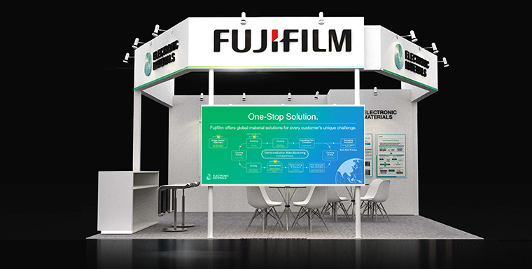
At SEMICON Southeast Asia 2026, Fujifilm will showcase a comprehensive lineup of semiconductor materials covering nearly the entire semiconductor manufacturing process, from cutting-edge to legacy nodes, as a “One-Stop Solution.”
Fujifilm will also introduce “ZEMATES™*1,” a brand of photosensitive insulating materials for semiconductor back-end processes, enhancing the reliability of semiconductor packaging.
With this extensive portfolio, Fujifilm aims to support the further growth of the rapidly expanding back-end market and the semiconductor industry in Southeast Asia, including neighboring countries such as Vietnam.
The semiconductor market in Southeast Asia is rapidly growing against the backdrop of supply chain diversification, with Singapore, where front-end companies such as memory manufacturers and foundries are concentrated, and Malaysia, which has established itself as a global hub for back-end processes, gaining attention as key hubs.
Recently, construction has begun on a new factory for a major memory manufacturer in Singapore, while in Malaysia, capital investments for back-end equipment by global semiconductor companies and OSAT (Outsourced Semiconductor Assembly and Test) providers have been accelerating. Additionally, investments related to power semiconductors are expanding to support production bases for final products such as automobiles and PCs within the region. The market is expected to experience continued mid- to long-term growth.
Fujifilm offers a comprehensive range of front-end materials, including photoresists*2 and CMP slurries*3, as well as back-end materials such as the photosensitive insulating material “ZEMATES™,” and is focusing its efforts on the Southeast Asian market to support the growing demand for a wide variety of semiconductors.
At “SEMICON Southeast Asia 2026,” Fujifilm will showcase its reliable semiconductor materials designed to support the growth of its customers in Southeast Asia.
The main exhibits are as follows.
- Photolithography solutions
EUV, ArF KrF and legacy resist, PFAS-free*4 resists, along with positive-tone developers such as TMAH, NTI developers*5, and photolithography-related materials*6 including etchants and cleaners. - CMP solutions
World-leading CMP slurries, including copper interconnect solutions, buffing cleaner*7 and post-CMP cleaners*8 - Process Chemicals*9
High Purity Process Chemicals such as straight acids bases and IPA. - Advanced packaging materials
“ZEMATES™” brand polyimides*10, thermal interface materials (TIM) and CMP slurries for advanced packaging
In October 2023, Fujifilm acquired the semiconductor process chemicals business of Entegris, Inc. (headquartered in Massachusetts, U.S.), a semiconductor materials manufacturer, thereby establishing its first production base in Southeast Asia, in Singapore, for its semiconductor materials business.
In addition to “local production for local consumption” strategy, manufacturing near Fujifilm’s semiconductor device manufacturer customers, Fujifilm has been strengthening a “local support” framework by applying its expertise in production, inspection technology, and quality assurance processes to their development, production, and quality control efforts.
Fujifilm will also introduce its product development and service infrastructure for advanced semiconductors tailored to the needs of the Southeast Asian market, and further strengthen its collaboration with local customers.
Fujifilm will continue its technological development and accelerate the provision of One-Stop Solution meeting diverse customer needs, thereby contributing to the further advancement of the global semiconductor industry.
- *1 ZEMATES is a registered trademark or trademark of FUJIFILM Corporation.
- *2 Photosensitive material used to coat a wafer substrate when circuit patterns are drawn using photochemical reactions in the process of semiconductor manufacturing.
- *3 A proprietary formulation containing an abrasive that uniformly planarizes semiconductor surface, which contains a mixture of wires and insulation films of varying hardness.
- *4 PFAS refers to a collective term for perfluoroalkyl compounds, polyfluoroalkyl compounds, and their salts, as defined in the OECD's 2021 report “Reconciling Terminology of the Universe of Per- and Polyfluoroalkyl Substances: Recommendations and Practical Guidance.” Accordingly, the claim ‘PFAS-Free’ denotes the absence of substances falling within this defined group.
- *5 Negative Tone Imaging (NTI) developer. It is used in the negative development process where the unexposed areas are removed by the developer after exposure to create the circuit pattern.
- *6 Development solutions, cleaners and other materials used in the photolithography process of semiconductor manufacturing
- *7 A cleaner that performs a pre-cleaning process on the platen after polishing with CMP slurry to enhance cleaning performance at the most advanced node
- *8 Cleaners used after polishing with CMP slurry to remove particles, minute metal fragments and organic residues while protecting the metal surface.
- *9 High-purity chemicals used in the cleaning and drying processes. The chemicals are employed to remove contaminants during the cleaning and drying stages of semiconductor manufacturing, as well as to eliminate metals and oils during the etching process.
- *10 A material with strong heat resistance and insulation properties, used for forming semiconductors’ protective films and redistribution layer.
- Date
May 5th to 7th, 2026
- Location
MITEC, Kuala Lumpur, Malaysia
- Booth No.
Hall 1 Booth No.:1122
- Exhibit Contents
Photoresists, Photolithography-related materials, CMP slurries, post-CMP cleaners, Advanced packaging solutions (such as polyimides and thermal interface materials under the “ZEMATES™” brand), etc.
Kompleks MITEC No.8, Jalan Dutamas 2 50480 Kuala Lumpur, Malaysia
FUJIFILM Holdings Corporation
Corporate Communications Division, Public Relations Group
Semiconductor Materials
FUJIFILM Corporation
Electronic Materials Business Division
- * Please note that the contents including the product availability, specification, prices and contacts in this website are current as of the date of the press announcement and may be subject to change without prior notice.