



TOKYO, August 21, 2026 – FUJIFILM Corporation today announced the completion of a new production building for post-CMP cleaners at the Oita Factory of FUJIFILM Electronic Materials Co., Ltd. (FFEM), the core company leading Fujifilm’s semiconductor materials business. The facility began operations in August. This investment will significantly expand production capacity for post-CMP cleaners used in the manufacturing of advanced semiconductors, including those for AI applications, for which demand is growing rapidly. Fujifilm will further accelerate the growth of its semiconductor materials business to meet the rising demand for semiconductors supporting the advanced information society, including semiconductors for AI data centers and other applications.
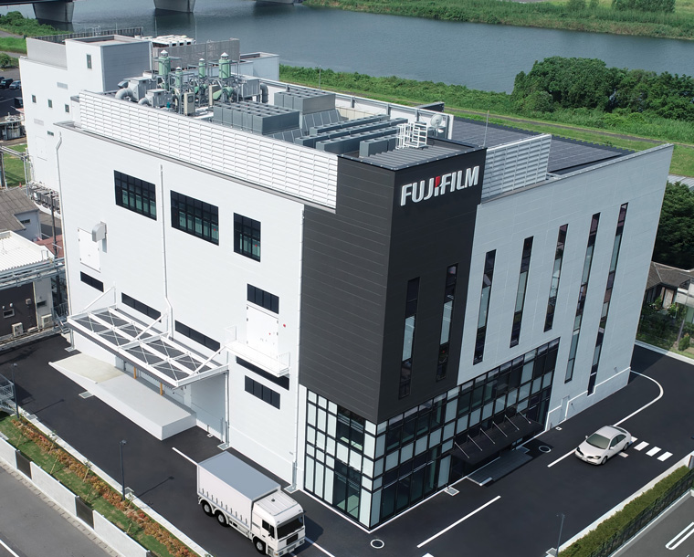
Exterior Photo of New Production Building
In recent years, the semiconductor market has grown rapidly driven by the expansion of AI, 5G, and IoT, with particularly strong demand for advanced semiconductors used in AI applications. Fujifilm’s semiconductor materials business achieved an average annual sales growth rate of approximately 20% from FY2021 through FY2025 and has become one of the core businesses driving the growth of the Fujifilm Group. To support this growth, Fujifilm invested more than 100 billion yen from FY2021 to FY2024. For example, the company expanded production capacity for CMP slurries*2 in Japan, the United States, and Taiwan, and CMP slurries have become one of the key products driving business growth. Fujifilm has also increased production capacity for polyimides*3 in Japan and Belgium, while demand for its photosensitive dielectric materials for advanced packaging, including ZEMATES™*4, has grown rapidly. The company continues to make growth investments across Japan, the United States, Europe, and Asia during FY2025 and FY2026, and will continue supporting the growth of the semiconductor market by providing a broad lineup of products.
The post-CMP cleaners manufactured at the Oita Factory are used after CMP processes to remove particles, trace metals, and organic residues while protecting metal surfaces. Demand is rapidly increasing not only for CMP slurries, which are essential for planarization processes required to improve semiconductor performance, but also for post-CMP cleaners used in subsequent cleaning processes. Leveraging its strength in providing integrated solutions incorporating both CMP slurries and post-CMP cleaners, Fujifilm is expanding sales globally, particularly among customers in North America, Europe, and key semiconductor manufacturing hubs in Asia, where demand growth in the advanced semiconductor market remains strong.
Driven by advancements in semiconductor miniaturization and 3D stacking technologies required to improve the performance of AI semiconductors, demand for Fujifilm’s post-CMP cleaners, which play a critical role in semiconductor manufacturing yield, is expected to more than double in terms of sales by FY2030 compared with FY2024. The new production building is equipped with automated manufacturing facilities and quality evaluation equipment designed to meet the extremely high purity requirements of cutting-edge semiconductor materials. By tripling production capacity at the Oita Factory, Fujifilm aims to further expand its business in the advanced semiconductor market.
Solar panels have been installed on the roof of the new building. Through greater use of renewable energy at the Oita Factory, Fujifilm will reduce greenhouse gas emissions generated by factory operations.
Fujifilm offers a wide range of materials used throughout the entire semiconductor manufacturing process, from front-end to back-end. These materials include photoresists*5, photolithography-related materials*6, CMP slurries, post-CMP cleaners, thin-film materials*7, photosensitive insulating materials such as polyimides under the ZEMATES™ brand, and high-purity process chemicals*8. Fujifilm also provides Wave Control Mosaic™*9, a group of functional materials including color filter materials for image sensors. With an extensive portfolio covering semiconductor manufacturing processes from leading-edge to legacy nodes, Fujifilm maintains a global supply chain with manufacturing and research and development sites in Asia, the United States, and Europe. By providing a one-stop solution to address customer needs, the company contributes to the advancement of the semiconductor industry.
- *1 Cleaners used after polishing with CMP slurry to remove particles, minute metal fragments and organic residues while protecting the metal surface.
- *2 A proprietary formulation containing an abrasive that uniformly planarizes semiconductor surface, which contains a mixture of wires and insulation films of varying hardness.
- *3 A material with strong heat resistance and insulation properties, used for forming semiconductorsprotective films and rewiring layer.
- *4 ZEMATES is a registered trademark or trademark of FUJIFILM Corporation.
- *5 Photosensitive material used to coat a wafer substrate when circuit patterns are drawn using photochemical reactions in the process of semiconductor manufacturing.
- *6 Development solutions, cleaners and other materials used in the photolithography process of semiconductor manufacturing.
- *7 Materials for forming low-dielectric insulation films.
- *8 High-purity chemicals used in the cleaning and drying processes. The chemicals are employed to remove contaminants during the cleaning and drying stages of semiconductor manufacturing, as well as to eliminate metals and oils during the etching process.
- *9 General term referring to a group of functional materials for controlling electromagnetic light waves in a broad range of wavelengths, including photosensitive color materials for manufacturing color filters for image sensors such as CMOS sensors, used in digital cameras and smartphones. WAVE CONTROL MOSAIC is a registered trademark or trademark of FUJIFILM Corporation.
- Location
3410-2 Nakanoshinchi, Oaza Shimogori, Oita City, Oita Prefecture (within FFEM Oita Factory)
- Total Floor Area
Approximately 3,600 m²
- Structure
Steel frame
- Floors
4 above ground
- Start of Operation
August 2026
- Total investment value
Approximately 7 billion yen (including building and equipment)
- Description
Production and quality inspection of post-CMP cleaners; office space
FUJIFILM Holdings Corporation
Corporate Communications Division, Public Relations Group
FUJIFILM Corporation
Electronic Materials Business Division
- * Please note that the contents including the product availability, specification, prices and contacts in this website are current as of the date of the press announcement and may be subject to change without prior notice.