


Enabling the semiconductor
evolution.
FUJIFILM-shaping
the future with materials.
FUJIFILM will be exhibiting at SEMICON JAPAN 2025.

Concept Video
Event Overview

- Date:December17(Wed) –19(Fri)
- Venue:Tokyo Big Sight
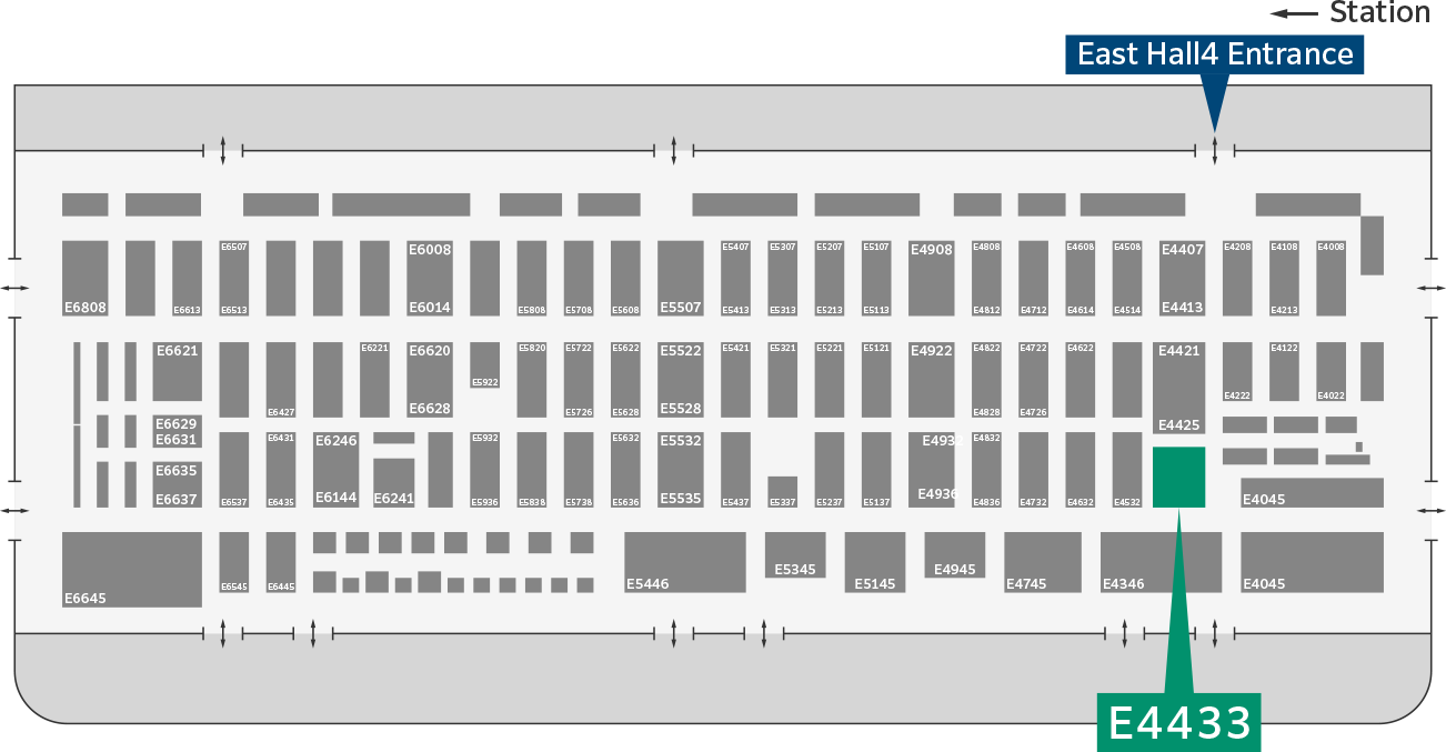
MAP - Booth No. E4433
[Register to attend]
Talk Overview
Next-Generation Semiconductor Manufacturing driven by the Cutting-Edge Materials with AI Co-Creation
- Fujifilm develop “one-stop solution” strategy, providing all customers a wide range of advanced materials and technical support across virtually all manufacturing processes, not only front-end but also back-end. This presentation will cover our unique business strategy, key product features, examples of AI collaboration model with customers and partners, and contributions to next-generation semiconductor manufacturing through ultra-advanced materials.
- Date & Time:December17(Wed) 16:00–16:30
- Venue:SuperTHEATER (West Hall 4)
- Tetsuya Iwasaki
Director, Senior Corporate Vice President
General Manager of
Electronic Materials Business Division
Global President of
FUJIFILM Electronic Materials


Exhibition Booth Overview
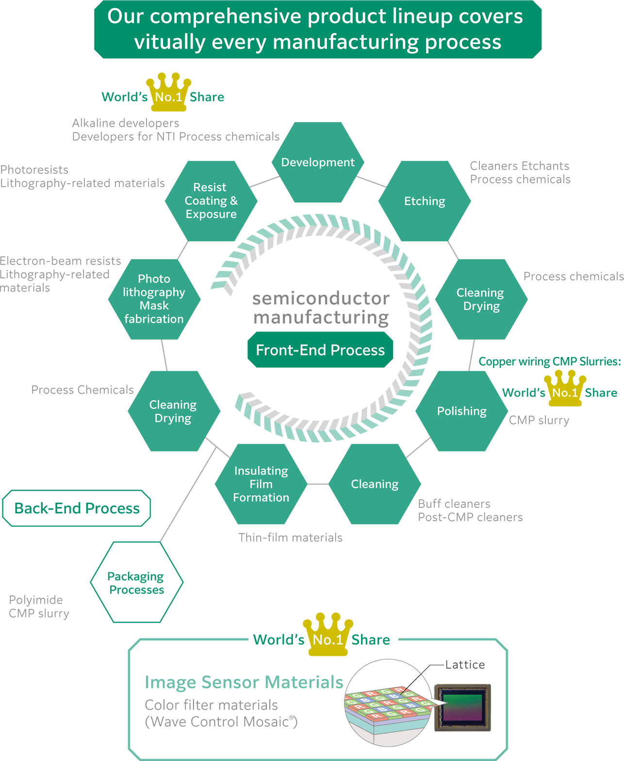
What “One-Stop Solution”
Means
-
1.Developing and supplying end to end materials
across the entire semiconductor
manufacturing process.
Delivering integrated solutions to
complex customer challenges
that can’t be solved by any single material alone.
Offering materials optimized for multiple
adjacent processes, all in one package. -
2.Providing optimal materials
for every type of semiconductor.
To every challenge— a solution.
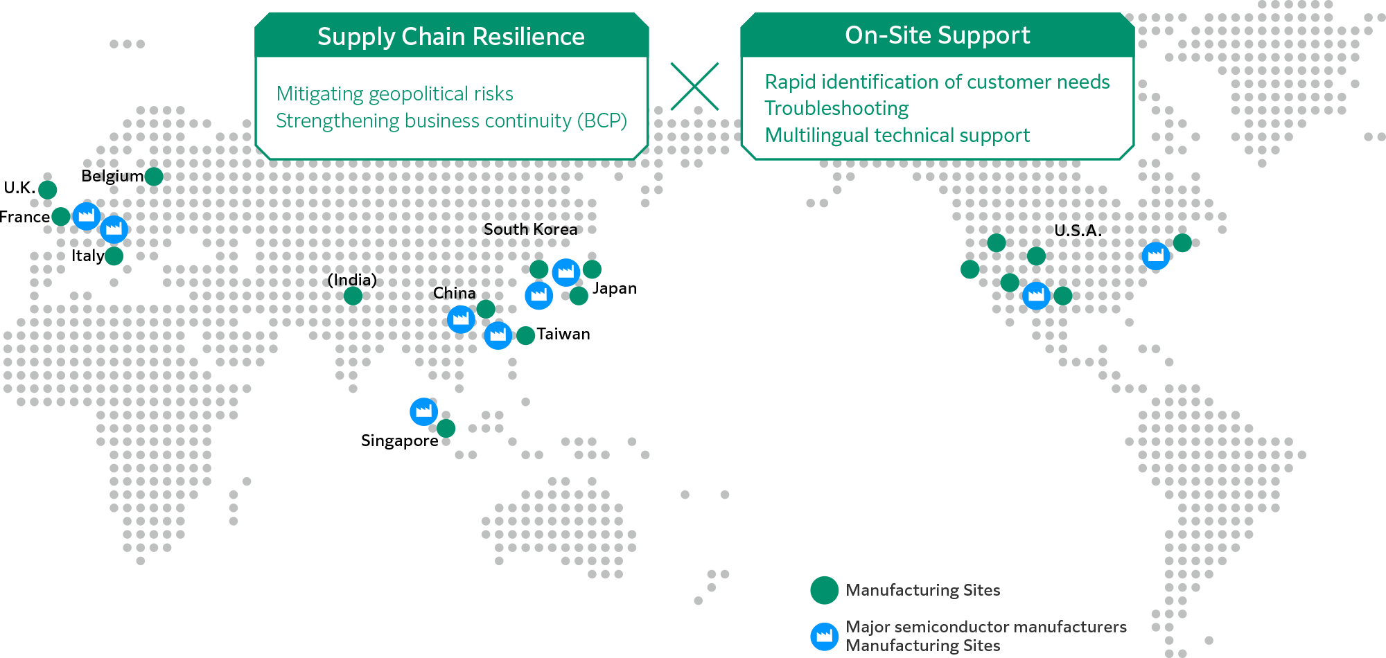
A Global Network
Close to Every Customer
A global network of production and R&D sites
Promoting next-generation process technology
and co-development of new products
with our customers.
Through a “local production for local consumption, local support”
framework,
we deliver solutions
precisely aligned with customer needs.
Product introduction
FFEM offers a wide product lineup covering
wafer processing to
advanced packaging
applications.
[Development of Current Products]
Leading the global CMP market with the best total
solution,
powered by expertise in polishing and cleaning.
- ・CMP Slurry
- ・pCMP Cleaner
- ・CMP for Hybrid Bonding
- ・CMP for Back End process
The Color Filter Materials with the world's largest market share for Image Sensors :
Go Beyond the
Limit of high Resolution, good Color Reproduction by New Technologies.
- ・WCM(Wave Control Mosaic®)
High Performance and High Quality Polyimide material, Resilient Supply Chain with Multiple Production Sites
- ・Liquid Type Polyimide : Low Temperature Cure, High Resolution, Good Mechanical Properties, Low Shrinkage, High Reliability
- ・Film Type Polyimide : Achieving an Excellent Planarity with Film Laminating Process
EUV NTD Resist Enabling High Resolution
- ・EUV Resist
- ・EUV Negative Tone Development System
[Solving Social Issues:Reducing Environmental Impact]
PFAS-Free Advanced Resist
- ・ArF
Heat Dissipation Materials
- ・TIM (Thermal Conductive Sheet)
Nanoimprint Technology Enabling
nano-patterning with Low Energy consumption
- ・Nanoimprint Lithography Technology
[Digital × Materials]
- ・Co-creation development utilizing materials informatics and generative AI
Contact
Media Contact
FUJIFILM Holdings Corporation
Corporate Communications Division,
Public Relations Group
TEL:+81-3-6271-2000
Business Contact
FUJIFILM Corporation
Electronic Materials Business Division
E-mail:shm-ff-em_inquiries@fujifilm.com