



TOKYO, August 27, 2026 – Fujifilm Corporation announces that its Taiwan-based semiconductor materials subsidiary, FUJIFILM Electronic Materials (Taiwan) Co., Ltd. (FETW) will exhibit at “SEMICON Taiwan 2026,” an international exhibition of semiconductor manufacturing equipment and materials, to be held in Taipei, Taiwan, from September 2 to 4, 2026.
At SEMICON Taiwan 2026, the company will present its extensive lineup of semiconductor materials covering a wide range of semiconductor manufacturing processes from cutting-edge to legacy nodes as a “one-stop solution.” In addition, Fujifilm will showcase its world-leading copper interconnect CMP slurry*1 and post-CMP cleaner*2 as well as the “ZEMATES™”*3 series of photosensitive insulating film materials for advanced packaging, which is currently experiencing rapid growth, particularly for AI semiconductors.
In Taiwan, one of the driving forces of the global semiconductor industry, Fujifilm continues to expand its presence as a partner in creating cutting-edge semiconductors while further strengthening its relationships of trust with its customers.
FETW is celebrating its 30th anniversary this year since its founding in 1996. Over the past 30 years, FETW has contributed to the development of the semiconductor industry in Taiwan—one of the world’s leading advanced semiconductor markets—through the development and stable supply of high-quality materials. Guided by a strong customer-first philosophy, FETW has pursued product development and manufacturing that anticipates customer needs, supporting the growth of the semiconductor industry not only in Taiwan but around the world. Over the past decade (2015–2025), FETW has achieved annual growth exceeding 15%, and its revenue has more than quadrupled.
To drive further growth, FETW plans to complete construction of a new plant in Hsinchu, Taiwan, in December 2026. This new plant will serve as the core facility of its Taiwan headquarters, consolidating R&D, manufacturing, and logistics functions for advanced semiconductors, and will be the largest facility in its semiconductor materials business.
This investment will further strengthen its business foundation in Taiwan and expand its supply system for advanced semiconductor materials, such as CMP slurries and post-CMP cleaners.
Moving forward, the company will continue to promote development, production, and quality control close to its customers and further strengthen its “local production for local consumption with local support” framework to contribute to the development of the global semiconductor industry from Taiwan.

Image of the new factory in Hsinchu, Taiwan
Fujifilm will continue to advance technological development and accelerate the provision of one-stop solutions that meet the diverse needs of customers, thereby contributing to the further development of the global semiconductor industry.
- Event Dates
September 2 – 4, 2026
- Venue
Taipei Nangang Exhibition Center (TaiNEX) Halls 1 and 2, Taipei, Taiwan
- Booth Number
L0316
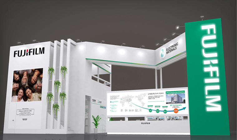
- Advanced Packaging Solutions
Advanced packaging materials, including “ZEMATES™” brand polyimides*4, thermal interface materials (TIM), and CMP slurries for advanced packaging - CMP Process Solutions
CMP slurries, buff cleaners, and post-CMP cleaners - Solutions for Image Sensors
“Wave Control Mosaic™”*5, featuring the world’s first color filter material for image sensors compatible with KrF exposure
- *1 A proprietary formulation containing an abrasive that uniformly planarizes semiconductor surface, which contains a mixture of wires and insulation films of varying hardness. CMP stands for Chemical Mechanical Polishing.
- *2 Cleaners used after polishing with CMP slurry to remove particles, minute metal fragments and organic residues while protecting the metal surface.
- *3 ZEMATES is a registered trademark or trademark of FUJIFILM Corporation.
- *4 A material with strong heat resistance and insulation properties, used for forming semiconductors’ protective films and redistribution layer.
- *5 General term referring to a group of functional materials for controlling electromagnetic light waves in a broad range of wavelengths, including photosensitive color materials for manufacturing color filters for image sensors such as CMOS sensors, used in digital cameras and smartphones. WAVE CONTROL MOSAIC is a registered trademark or trademark of FUJIFILM Corporation.
FUJIFILM Holdings Corporation
Corporate Communications Division, Public Relations Group
FUJIFILM Corporation
Electronic Materials Business Division
- * Please note that the contents including the product availability, specification, prices and contacts in this website are current as of the date of the press announcement and may be subject to change without prior notice.