


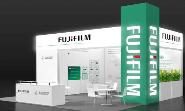
TOKYO, November 5, 2026- FUJIFILM Corporation announced that its European subsidiary for semiconductor materials, FUJIFILM Electronic Materials (Europe) N.V., will exhibit at “SEMICON Europa 2026,” to be held in Munich, Germany, from November 10 to 13, 2026.
The European semiconductor market has developed with its own distinct characteristics, with a particular strength in semiconductors for the automotive and industrial equipment sectors. Furthermore, in accordance with the European Chips Act, efforts are underway to expand production capacity within the region and strengthen the supply chain, and the European semiconductor market is expected to continue growing over the medium to long term.
In this market environment, expectations are rising for semiconductor materials manufacturers to ensure a stable, regional supply of high-quality, cutting-edge semiconductor materials. With bases located close to customers in Belgium, France, the United Kingdom, and Italy, Fujifilm has supplied high-quality semiconductor materials to major European semiconductor manufacturers and global semiconductor manufacturers with production bases in Europe through “one-stop solutions” that leverages the company’s extensive product lineup covering a wide range of semiconductor manufacturing processes. Fujifilm’s “local production for local consumption with local support” system—which allows quick identification of market trends and customer needs while resolving challenges and ensuring a stable supply—is a key strength of the company and is highly valued by customers.
Furthermore, with an eye toward market growth and expanding customer demand, Fujifilm continues to invest in its production and development infrastructure in Europe. At the FUJIFILM Electronic Materials (Europe) regional headquarters in Belgium, it has expanded production capacity for photolithography-related materials*1, while also proceeding with the expansion of production capacity for polyimide*2—where sales have grown significantly against the backdrop of market growth—and the introduction of new CMP slurry*3 production equipment. By gradually bringing these facilities online in response to customer demand trends and further strengthening supply capacity for advanced semiconductor materials within Europe, Fujifilm will contribute to customers’ growth and the development of the semiconductor industry, while also driving business growth.
“Our strength lies in the range of materials we offer, enabling us to provide semiconductor manufacturers with a one-stop solution. In addition to our global supply chain, we have a strong local supply chain in Europe, allowing us to respond to our customers’ evolving needs” — Hans Vloeberghs, President & Managing Director of FUJIFILM Electronic Materials (Europe) N.V.
At SEMICON Europa, Fujifilm will showcase its product portfolio, which comprehensively covers semiconductor manufacturing processes, with the aim of further strengthening its presence in the European semiconductor market. In particular, materials for advanced packaging—for which demand is growing as AI semiconductors become more powerful— will be on show, as well as environmentally friendly materials, which are attracting increasing interest in the European market.
In the advanced packaging area, Fujifilm will showcase a wide range of process materials, centered on its ZEMATES™*4 brand of photosensitive dielectric materials. As semiconductor packages become larger, denser, and generate more heat, there is a growing need for advanced materials that meet increasingly demanding requirements, including fine-pitch patterning, warpage control, narrow-gap filling, heat dissipation, and thermal conductivity.
In terms of environmentally friendly materials, Fujifilm has achieved a PFAS-free*5 lineup across the entire “ZEMATES™” product range and will introduce a PFAS-free negative-type ArF immersion resist for advanced semiconductors.
Moving forward, Fujifilm will continue to meet the needs of the European market—such as strengthening regional supply chains and promoting environmentally friendly practices—through a product lineup that broadly covers semiconductor manufacturing processes and stable supply leveraging its global “local production for local consumption with local support” framework. Fujifilm is committed to contributing to the development of the semiconductor industry in Europe and around the world.
- Event Dates
November 10 (Tue) – 13 (Fri), 2026
- Venue
Messe München (Munich, Germany)
- Booth Number
Hall B1, Booth 516
- *1 Development solutions, cleaners and other materials used in the photolithography process of semiconductor manufacturing.
- *2 A material with strong heat resistance and insulation properties, used for forming semiconductors’ protective films and redistribution layer.
- *3 A proprietary formulation containing an abrasive that uniformly planarizes semiconductor surface, which contains a mixture of wires and insulation films of varying hardness. CMP stands for Chemical Mechanical Polishing.
- *4 ZEMATES is a registered trademark or trademark of FUJIFILM Corporation.
- *5 PFAS refers to a collective term for perfluoroalkyl compounds, polyfluoroalkyl compounds, and their salts, as defined in the OECD's 2021 report “Reconciling Terminology of the Universe of Per- and Polyfluoroalkyl Substances: Recommendations and Practical Guidance.” Accordingly, the claim ‘PFAS-Free’ denotes the absence of substances falling within this defined group.
FUJIFILM Holdings Corporation
Corporate Communications Division, Public Relations Group
FUJIFILM Corporation
Electronic Materials Business Division
- * Please note that the contents including the product availability, specification, prices and contacts in this website are current as of the date of the press announcement and may be subject to change without prior notice.