


![[icon] Healthcare IT](https://asset.fujifilm.com/www/my/files/2024-08/8c54e70584c4081f9a826d25413251b5/healthcare-it.svg)
![[icon] X-ray](https://asset.fujifilm.com/www/my/files/2024-08/16de5a31d007bbcae6897896cea0180b/x-ray.svg)
![[icon] Ultrasound](https://asset.fujifilm.com/www/my/files/2024-08/f8411c9bbcc092e69403002d8ec87a2f/ultrasound.svg)
![[icon] Endoscopy](https://asset.fujifilm.com/www/my/files/2024-08/e546ad6bda4d6e375259635b639243a3/endoscopy.svg)
![[icon] In Vitro Diagnostics](https://asset.fujifilm.com/www/my/files/2024-08/45651a1911054d0278aff75e47c62a5f/ivd.svg)
![[icon] Veterinary Medicine](https://asset.fujifilm.com/www/my/files/2024-08/83f5645145bba7afca1a8f71b3729a12/veterinary.svg)
![[icon] MRI and CT](https://asset.fujifilm.com/www/my/files/2024-08/a4c4b5f9cc7e13e1b0ca0d9f7b2f7e4c/mri-and-ct.svg)
![[icon] Inkjet Solutions](https://asset.fujifilm.com/www/my/files/2024-08/7032541b9fb5f48f7128c4d0f0151619/inkjet-solutions.svg)
![[icon] Office Solutions](https://asset.fujifilm.com/www/my/files/2024-08/c0e0aa6e4964be7a6526a23000fa32dc/office.svg)
![[icon] Semiconductor Materials](https://asset.fujifilm.com/www/my/files/2024-08/66f74cc6c187695b6e5b881e283189f4/semconductor-materials.svg)
![[icon] Graphic Arts & Printing](https://asset.fujifilm.com/www/my/files/2024-08/d6b1a32f1e845c70ec5d17a004624e9f/graphic.svg)
![[icon] Photofinishing Products](https://asset.fujifilm.com/www/my/files/2024-08/ee9703dbf24f6be4e3df1ae9b445174f/photofinishing.svg)
![[icon] Optical Devices](https://asset.fujifilm.com/www/my/files/2024-08/b038cdcb48c672de30ab7e0224f3516f/optical-devices.svg)
![[icon] Cine & Broadcast Products](https://asset.fujifilm.com/www/my/files/2024-08/1a15109efbf16cae12a2a437b1c54541/film-and-broadcast.svg)
![[icon] Security Protections](https://asset.fujifilm.com/www/my/files/2024-08/d8dee0abf398463bd1564573f8c24960/security.svg)
![[icon] Manufacturing Process](https://asset.fujifilm.com/www/my/files/2024-08/310ce3db7347bb327992d312f9e18efd/manufacturing-process.svg)
![[icon] Inspectional Products](https://asset.fujifilm.com/www/my/files/2024-08/bc8914dd37045e60b0e03e5534138f35/inspection.svg)
![[icon] Data Management](https://asset.fujifilm.com/www/my/files/2024-08/32d8997a781b7095a93d31cdca37e80b/data-management.svg)
![[icon] Materials](https://asset.fujifilm.com/www/my/files/2024-08/8a30ec1d1fa7bd86f00f15d80e34e801/materials.svg)


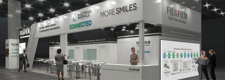
TOKYO, February 4, 2026 – FUJIFILM Corporation will participate in “SEMICON Korea 2026”, an international exhibition of semiconductor manufacturing equipment and materials, to be held in, Seoul, Korea, from February 11 to 13, 2026.
South Korea is home to major semiconductor manufacturers producing advanced memory, advanced logic, for which demand is growing due to the expansion of AI servers , and image sensors. Fujifilm is expanding sales of a wide range of advanced semiconductor materials to these semiconductor manufacturers, including advanced photoresists*1 (such as EUV resists), CMP slurries*2, polyimides*3, and color filter materials for image sensors. Fujifilm introduces its broad portfolio of cutting-edge semiconductor materials as a “one-stop solution,” demonstrating its robust local production and support capabilities to contribute to the further advancement of the semiconductor industry in South Korea and worldwide.
At SEMICON Korea 2026, Fujifilm will showcase a comprehensive lineup of semiconductor materials covering nearly the entire semiconductor manufacturing process, from cutting-edge to legacy nodes. Fujifilm will also introduce new products of its world-leading image sensor color filter material “WAVE CONTROL MOSAIC™*4” and “ZEMATES™*5,” a new brand of photosensitive insulating film materials for back-end processes that contribute to improving semiconductor package reliability.
The main exhibits are as follows.
- Photolithography solutions
EUV, ArF KrF and legacy resist, PFAS-free*6 resists, nanoimprint*7 resists, along with positive-tone developers such as TMAH, NTI developers*8, and photolithography-related materials*9 including etchants and cleaners. - CMP solutions
World-leading CMP slurries including copper interconnect solutions, buffing cleaner*10 and post-CMP cleaners*11 - Process Chemicals*12
High Purity Process Chemicals such as straight acids bases and IPA. - Advanced packaging materials
“ZEMATES™” brand polyimides and thermal interface materials (TIM) - Image sensor color filter materials
WAVE CONTROL MOSAIC™, including the world's first KrF-compatible image sensor color filter material
This extensive portfolio positions Fujifilm as a trusted partner for customers seeking comprehensive, dependable, and innovative material solutions across the entire semiconductor value chain.
In addition to its existing facility in Cheonan, South Korea, Fujifilm commenced operations at a new plant in Pyeongtaek in December 2024. This expansion advances its “local production for local consumption” strategy by enabling manufacturing closer to its semiconductor device manufacturers, while also strengthening a “local support” framework to assist customers in development, production, and quality management from nearby locations.
In 2025, Fujifilm received the “Most Valuable Partner Award” from Samsung Electronics Co., Ltd. (Headquarters: South Korea; hereinafter Samsung Electronics), the highest recognition for semiconductor material suppliers. The award recognizes Fujifilm’s contribution to the growth of Samsung Electronics' semiconductor business by solving its challenges through the supply of a wide range of advanced semiconductor materials, the establishment of production bases near customers to ensure consistent, high-quality product supply, and the provision of rapid on-site support.
Fujifilm will continue its technological development and accelerate the provision of one-stop solutions that meet diverse customer needs, thereby contributing to the further advancement of the global semiconductor industry.
- Date
February 11th to 13th, 2026
- Location
COEX, Seoul, Korea, Hall D, BoothNo:DS40
- Exhibit Contents
- Photoresists(EUV, ArF, KrF, legacy, PFAS-free resists, nanoimprint resists)
- CMP Solutions (CMP slurry/post-CMP cleaner, etc.)
- Process Chemicals
- Advanced packaging materials (Polyimide under the “ZEMATES™” brand, thermal management materials, etc.)
- Color filter materials for image sensors (New product WAVE CONTROL MOSAIC™ compatible with KrF exposure, etc.)
513, Yeongdong-daero, Gangnam-gu
Seoul 06164 Republic of Korea
- *1 Material used to coat wafer substrate when circuit patterns are drawn in the process of semiconductor manufacturing.
- *2 A proprietary formulation containing an abrasive that uniformly planarizes semiconductor surface, which contains a mixture of wires and insulation films of varying hardness.
- *3 A material with strong heat resistance and insulation properties, used for forming semiconductors’ protective films and redistribution layer.
- *4 General term referring to a group of functional materials for controlling electromagnetic light waves in a broad range of wavelengths, including photosensitive color materials for manufacturing color filters for image sensors such as CMOS sensors, used in digital cameras and smartphones. WAVE CONTROL MOSAIC is a registered trademark or trademark of FUJIFILM Corporation.
- *5 ZEMATES is a registered trademark or trademark of FUJIFILM Corporation.
- *6 PFAS refers to a collective term for perfluoroalkyl compounds, polyfluoroalkyl compounds, and their salts, as defined in the OECD's 2021 report “Reconciling Terminology of the Universe of Per- and Polyfluoroalkyl Substances: Recommendations and Practical Guidance.” Accordingly, the claim ‘PFAS-Free’ denotes the absence of substances falling within this defined group.
- *7 Nanoimprint lithography. A technology in which a mask (mold) with circuit patterns is pressed onto the resist applied to a semiconductor wafer, like a stamp, to transfer and form the circuit patterns.
- *8 Negative Tone Imaging (NTI) developer. It is used in the negative development process where the unexposed areas are removed by the developer after exposure to create the circuit pattern.
- *9 Development solutions, cleaners and other materials used in the photolithography process of semiconductor manufacturing.
- *10 A cleaner that performs a pre-cleaning process on the platen after polishing with CMP slurry to enhance cleaning performance at the most advanced node.
- *11 Cleaners used after polishing with CMP slurry to remove particles, minute metal fragments and organic residues while protecting the metal surface.
- *12 High-purity chemicals used in the cleaning and drying processes. The chemicals are employed to remove contaminants during the cleaning and drying stages of semiconductor manufacturing, as well as to eliminate metals and oils during the etching process.
FUJIFILM Holdings Corporation
Corporate Communications Division, Public Relations Group
FUJIFILM Corporation
Electronic Materials Business Division
- * Please note that the contents including the product availability, specification, prices and contacts in this website are current as of the date of the press announcement and may be subject to change without prior notice.