


FUJIFILM Business Innovation's One-Pass Duplex Scanning Technology enables the simultaneous scanning of both sides of a document through a single pass of the scanning area of multifunction devices.
Compared to Three-Pass Duplex Scanning Technology (Fig. 2) in which a document is passed through the DADF scanner three times, One-Pass Duplex Scanning Technology saves more energy, employs a smaller DADF scanner, and minimizes damage to the original document.
One-Pass Duplex Scanning Technology posed a problem, however, in that the side 2 scanning area was easily affected by dirt and dust during document scanning. This resulted in the input of incorrect information.
FUJIFILM Business Innovation solved this problem using its exclusive Hybrid Shading Correction Technology. The side 2 scanning area consists of the Contact Image Sensor (CIS), facing the white reference plane in parallel. Before scanning a document, the CIS scans the white reference plane and collects the shading data necessary for Shading Correction Processing.*1 The white reference plane is easily affected by dirt and dust when a document passes between it and the CIS. Therefore, many areas of the white reference plane are normally scanned in terms of lines, and then the clean pixels of each line are selected to obtain shading data. In the past, such scanning of lines required a mechanical driver to shift the white reference plane. Hybrid Shading Correction Technology, however, needs no such mechanical driver and allows for a smaller DADF scanner and more energy-saving features. Specifically, Hybrid Shading Correction Technology enables the creation of shading data as follows: 1) a white sheet type plate in a clean condition is scanned beforehand, with the collected information being stored as standard data; 2) the white reference plane is scanned just prior to the scanning of each document, with this new data being merged with the standard data; and 3) by merging the two types of data, the newly developed correction technology is applied to create shading data.
Next, we introduce Between Chip Image Correction Technology used in the side 2 scanning area. In the CIS, CMOS chips are positioned in a single line array in the fast scan direction (perpendicular to the direction in which a document is transported). Due to manufacturing restrictions, the chips cannot be laid in a single line without having gaps occur at certain intervals, and areas of the document being fed under these gaps cannot be scanned. FUJIFILM Business Innovation's technology solved this problem and enabled image correction in the gaps between chips, by selecting similar images from the image information collected from areas adjacent to the gaps, and then using those selected images for correction (Fig. 3).
As described above, FUJIFILM Business Innovation's exclusive technology has yielded One-Pass Duplex Scanning Technology-one of the industry's most advanced technologies.
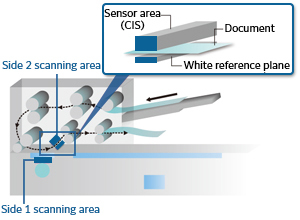
Fig. 1: One-Pass Duplex Scanning(for scanning both sides of a document in a single pass)
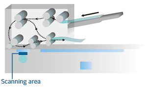
Fig. 2: Three-Pass Duplex Scanning The document is scanned three times: 1) Side 1 is scanned; 2) Side 2 is scanned; 3) The document is flipped over to its original position.
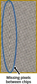
Fig. 3: Before Correction
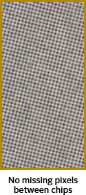
Fig. 3: After Correction
-
- *1 In order to correct per-pixel variations (e.g., sensitivity, amount of exposure to light) of the scanning sensor, a single line is scanned from the white reference plane beforehand, and then stored as standard shading data. When a document is scanned, the scanned image data is divided by the shading data for each pixel, thereby achieving evenness in scanning. As the ambient environment easily affects the scanning sensor, Shading Correction Processing is performed just prior to scanning a document.